


Features and applications of Inp wafers
2025-04-11
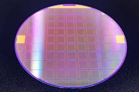
Features of InP wafer
InP wafers are composed of indium and phosphorus in a zinc-sulfur crystal structure with a density of about 4.81 g/cm³ and a melting point of 1062°C. It has high electron mobility and a direct band gap, which makes it excellent in high-speed electronic devices. Thermal conductivity and optical refractive index (about 3.1 in infrared) also support its use in optoelectronic applications.
Applications of InP wafers
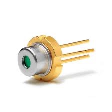
InP wafers are primarily used in optical communication devices such as laser diodes and light detectors to optimize fiber communication performance, especially at 1550 nm wavelengths. It is also used in high-frequency electronic devices such as microwave and millimeter-wave circuits, as well as solar cells and quantum computing. In addition, InP has potential in emerging areas such as lidar, the automotive industry, and pollution control, especially in industrial and medical sensing applications.

Detailed report
InP (Indium phosphide) wafer is a compound semiconductor material that plays an important role in high-performance electronic and optoelectronic devices due to its excellent electrical and optical properties. The following is a comprehensive analysis of InP wafer characteristics and applications, based on information from multiple sources, including commercial suppliers and academic sources, to ensure accuracy and comprehensiveness.
Features of InP wafer
The physical, electrical, and optical properties of InP wafers make them stand out in a variety of high-tech applications. Here is a detailed list of features:
* Chemical and crystal structure: InP is composed of indium (In) and phosphorus (P) with the chemical formula InP and molecular weight of 145.79 g/mol. The crystal structure is zinc-sulfur type (face-centered cubic) and the lattice constant is 0.58687 nm, which is consistent with the characteristics of III-V semiconductors such as GaAs.
* Physical Characteristics:
* Density: about 4.81 g/cm³ (source agreement is high, some commercial data is 4.787 g/cm³, may vary due to measurement conditions).
* Melting point: 1062°C (1944°F; 1335 K), suitable for high temperature processes.
* Color: gray-black crystal, medium mechanical hardness, chemically stable in air, insoluble in water.
* Electrical characteristics:
* Band gap: Direct band gap with a width of 1.344 eV (at 300 K), some sources mention 1.35 eV, which may be a difference in measurement temperature or method.
* Electron mobility: approximately 5400 cm²/(V·s) (at 300 K), some commercial data is 4600 cm²/(V·s), may vary due to doping or purity.
* Hole mobility: about 160 cm²/(V·s).
* Compared to silicon (Si) and gallium arsenide (GaAs), InP has higher electron velocity and lower base thin layer resistance with higher base electron diffusivity.
* Thermal characteristics:
* Thermal conductivity: about 0.68 W/(cm·K) (at 300 K), support efficient thermal management.
* Optical characteristics:
* Refractive index: about 3.1 in the infrared spectrum, about 3.55 at 632.8 nm wavelength, suitable for optoelectronic device design.
* High electro-optical conversion efficiency, making it excellent in the conversion of light and electric energy.
* Other key features:
* High operating temperature and strong radiation resistance, especially suitable for space and aviation applications.
* Good thermal conductivity, support high power device operation.
These characteristics make InP wafers particularly suitable for applications requiring high frequencies, high power, and photoelectric conversion efficiency
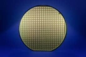
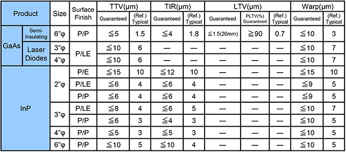
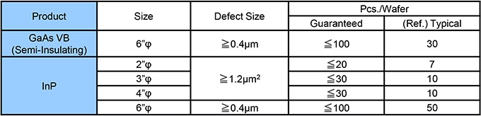
Dimensions and specifications of InP wafers
Applications of InP wafers
Applications for InP wafers range from traditional optical communications and high-frequency electronics to emerging technologies such as quantum computing and lidar. The following are detailed by category:
1. Optical communication:
InP is the core material of optical communication and is used in the manufacture of laser diodes, light-emitting diodes (LEDs) and Photodetectors.
Especially at the 1550 nm wavelength, InP devices are ideal for fiber communication because this band has the lowest fiber loss (about 0.2 dB/km), supports single-mode operation in the 1510-1600 nm range, and reduces inter-mode dispersion.
For 400Gbps and 800Gbps high-speed transceivers to meet the needs of data centers and telecommunications for high data rates (such as 100Gbps single InP lasers).
* Photonic Integrated Circuits are based on InP for generating, amplifying, controlling and detecting laser light, and support wavelength division multiplexing (WDM) technology.
2. High-frequency electronic devices:
InP is used to manufacture high electron mobility transistors (HEMTs) and heterojunction bipolar transistors (HBTS), which are widely used in microwave and millimeter wave circuits.
* Supports frequencies up to 604 GHz and is particularly suitable for high speed electronic applications such as satellite communications and wireless networks.
3. Solar Technology:
* InP is used to manufacture highly efficient solar cells, especially in space and aviation, due to their high radiation tolerance and high conversion efficiency.
4. Optoelectronic integrated circuit:
* InP is used as a substrate to manufacture integrated circuits that combine optical and electronic functions and is widely used in optical communication systems.
5. Quantum Computing:
* InP has potential in quantum computing, particularly in manufacturing qubits and photonic devices, to support future computing breakthroughs.
6. Photoelectric sensor:
* InP is used to manufacture photoelectric sensors for environmental monitoring, industrial inspection and medical diagnostics. For example, real-time detection of CO, CO₂, NOₓ in the air is used for pollution control.
7. Emerging applications:
In LiDAR, InP is used in the automotive industry (such as autonomous driving sensors), industrial, medical, defense, infrastructure, and agri-food sectors to detect food, plastics, and illicit drugs through non-destructive spectral analysis.
In mobile phone power amplifiers (PA) and wearable devices, InP has potential due to its high frequency performance.
* Also supports fiber to the home (FTTH) and data center communications to meet high-speed network requirements.
Market and production background
InP wafers are produced using a variety of growth methods, including liquid-sealed Czochra (LEC), vertical gradient solidification (VGF) and vertical Bridgman (VB), depending on crystal size, purity and performance requirements.
* Market size: The global InP wafer market sales in 2023 will reach billions of yuan, and it is expected to continue to grow in 2030, with a compound annual growth rate (CAGR) of a certain percentage (specific data need to refer to market reports, such as the Global Indium phosphide Wafer Industry Report 2024).
* Major manufacturers include Sumitomo Electric Industries, AXT, Wafer World Inc. The supply range covers N-type, P-type and semi-insulated wafers.
Summary and prospect
InP wafers are key materials for high-performance electronic and optoelectronic devices due to their excellent electron mobility, direct bandgap and optical properties. Its applications extend from traditional optical communications and high-frequency electronics to emerging fields such as quantum computing and lidar, particularly in fiber optic communications and optical sensing applications at 1550 nm wavelengths. In the future, with the improvement of device performance and size reduction, the quality requirements of InP wafers will be higher, and its market prospects are broad, especially in technology-driven industries such as 5G, artificial intelligence and autonomous driving


