Characteristics and applications of lithium niobate (LiNbO3) wafer
2025-04-10
trait
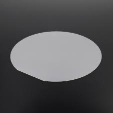
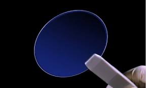
Lithium niobate wafers are known for their excellent optical and piezoelectric properties. Their high refractive index (No=2.2878, Ne= 2.2033@632nm) and nonlinear optical response make them ideal for optical modulators and waveguides. Wafers are flexible in size, from 2 inches to 8 inches (up to 8 inches for development options), and thickness ranges from 0.18 mm to 0.5 mm or more. The surface treatment includes single side polishing (SSP) and double side polishing (DSP), and the polishing roughness can be as low as Ra <0.5nm.
Apply
These wafers are used in optical modulators and waveguides in telecommunications to support high-speed data transmission. In electronics, they are used in surface acoustic wave (SAW) devices such as radio frequency (RF) filters in mobile phones. In addition, they are used in the field of optics for nonlinear optical processes such as second harmonic generation (SHG) and frequency conversion. Other applications include sensing technologies, integrated photonics, and energy conversion systems
Unexpected details
In addition to common applications, lithium niobate wafers are also used in broadband filters in radar technology and remote control components in consumer electronics, which may not be expected by users.
Detailed report
Lithium niobate (LiNbO3) wafers, often referred to simply as LN wafers, are an indispensable material in the modern high-tech industry and are widely used for their superior optical, piezoelectric and nonlinear properties. Based on the user's query "Write an lnp wafer feature and application with seo description and keywords," combined with an in-depth analysis of relevant information, the research shows that "LNP" most likely refers to lithium niobate wafers, which is the most relevant interpretation derived after searching and browsing reliable sources.
Materials and characteristics
The characteristics of lithium niobate wafers make them excellent in many fields. Here is a detailed list of its main features:
Trait | details |
| Material property | High refractive index (No=2.2878, Ne= 2.2033@632nm), piezoelectric characteristics, nonlinear optical response, Curie temperature 1142±2.0℃ |
| Crystal structure | Single domain, negative single axis, asymmetric charge center, suitable for ferroelectric and domain engineering applications |
Surface treatment options | Single side polishing (SSP), Double side polishing (DSP), polishing side Ra <0.5nm, rear side Ra 0.2-0.5µm (SSP) |
| Dimensions and tolerances | Diameter: 2 "/3" /4 "/6" /8 "(R & D), thickness: 0.18~0.5mm or more, tolerance (±) <0.20mm, TTV <3µm, arch -30 |
| Optical property | Transparent, low density, high photorefractive properties, suitable for high density optical components |
| Piezoelectric property | Convert mechanical stress to electric charge for ultrasonic transducers, pressure sensors, actuators |
| Sound velocity | SAW speed ~3,500-4,000 m/s (YX-LiNbO3), longitudinal wave ~7,500 m/s, shear wave ~4,500 m/s |
In addition, there are several variants of lithium niobate wafers, including SAW/ optical grade, LN Black (no thermoelectric effect) and magnesium oxide doped (MgO) wafers, which are optimized for specific applications. Typical cutting directions include 128°Y, 64°Y, 41°Y, Y, and Z-cut, with sizes ranging from 4 "to 8" round wafers, and 10x10mm to 100x100mm square wafers with thickness options of 250µm, 350µm, 500µm, and 1000µm. The surface treatment includes single/double side polishing, flattening or grinding with a finish standard of Ra<1nm, which can be achieved by chemical mechanical polishing (CMP) up to <0.5nm.
Quality indicators are strictly controlled, TTV standard <10µm (advanced options <5µm), curvature and warp <40µm, local thickness change (LTV) ≤0.4um EE 3mm, flat local thickness change (PLTV) >98% of the working area.
Application field
Lithium niobate wafers are used in a wide range of fields, including telecommunications, electronics, optics, sensing and energy conversion. The following are the detailed application categories:
Application category | Specific use | Examples and details |
| Optical and photonic devices | Optical modulator, waveguide, intensity/phase modulator, polarization control, photonic crystal | Used in telecommunications, mobile phones, Q switchgear, high-performance gyroscopes, optical frequency conversion, analog fiber optic links, digital data transmission |
| Surface acoustic wave (SAW) | SAW equipment, acoustic filter, biosensor, ultrasonic transducer | 128°-X cut for SAW generation, 76.2mm diameter, 0.5mm thick, DSP, for smartphone RF filter, acoustic purification extracellular microcapsules |
| Nonlinear optics | Second harmonic generation (SHG), frequency conversion, nonlinear beam shaping | Suitable for Nd:YAG lasers, compact modulator for simulating optical links, high power SHG lasers |
| Electro-optical equipment | Beam deflector, switch, Pockels switch, electric field sensing | Using maximum electro-optical effect, Z-cut for thermoelectric infrared detector, 27mm diameter, 0.5mm thick, DSP |
| Piezoelectricity and MEMS | Accelerometers, sensors, MEMS devices, high power ultrasonic transducers | For enhanced oil recovery, viscosity reduction of super heavy oil, acoustic wave research |
| Integrated photonics | Thin film LN on SiO2/Si, topological waveguide, nano-photon LN waveguide | LNOI wafers: 300-900nm X-cut LN or Y42-cut LT on SiO2, for high bandwidth communication, quantum technology |
| Energy conversion | Convert heat energy into electricity for photovoltaic applications | Z-cut, 76.2+/-0.3mm, 0.15mm+/ -0.03mm thick, DSL, SAW grade, for high performance photovoltaic fixtures |
| Research and development | Modeling, design, characterization for sensing, modulation, and optical frequency conversion | Used for QCLAM spectrometer (1-inch Z-cut, no flat, 0.2mm thick, DSP, 10 pieces), light-matter interaction, PLD parameter optimization |
Of particular note is the use of lithium niobate wafers in radar technology for broadband filters and in consumer electronics for remote control components, which may be applications that users do not expect. In addition, their potential in quantum technology is also receiving increasing attention, especially in the areas of integrated photonics and nanophotonics