From Crystal to Chip: The Manufacturing Process of SiC Wafers
2025-04-19
Overview of SiC Wafer Manufacturing
Youdaoplaceholder0 Silicon carbide (SiC) wafers are the core of high-power electronics, and their manufacturing process begins with crystal growth. The physical vapor transport (PVT) method is usually adopted to heat high-purity SiC powder to above 2000°C and form single crystal rods in a vacuum environment. This process takes several weeks and the quality of the crystal directly affects the final performance.
Detailed steps
1.Crystal growth: By using the PVT method, the SiC powder sublimates and condenses on the seed crystals to form crystal rods.
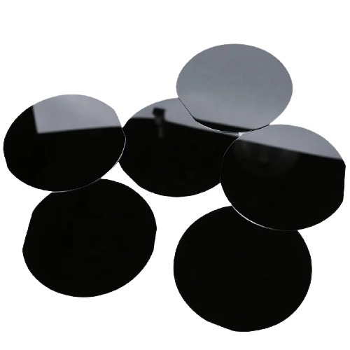
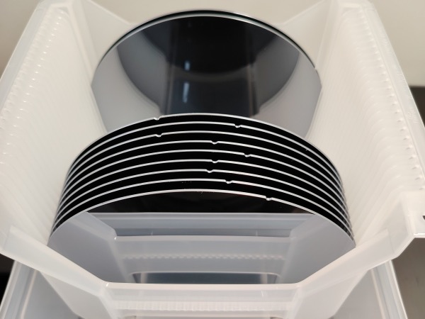
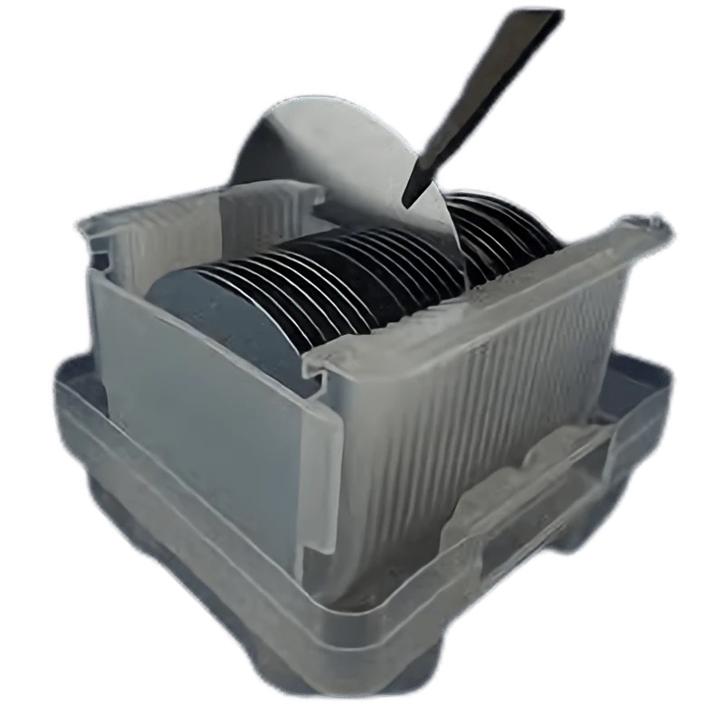
2. Wafer cutting: Use multi-wire cutting equipment to cut the crystal rods into thin slices with a thickness of no more than 1mm. The hardness and fragility of SiC pose challenges.
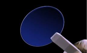
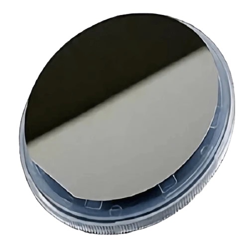
3. Grinding and polishing: The wafer is ground with diamond grinding fluid, followed by mechanical and chemical mechanical polishing to achieve a mirror-like smooth surface.
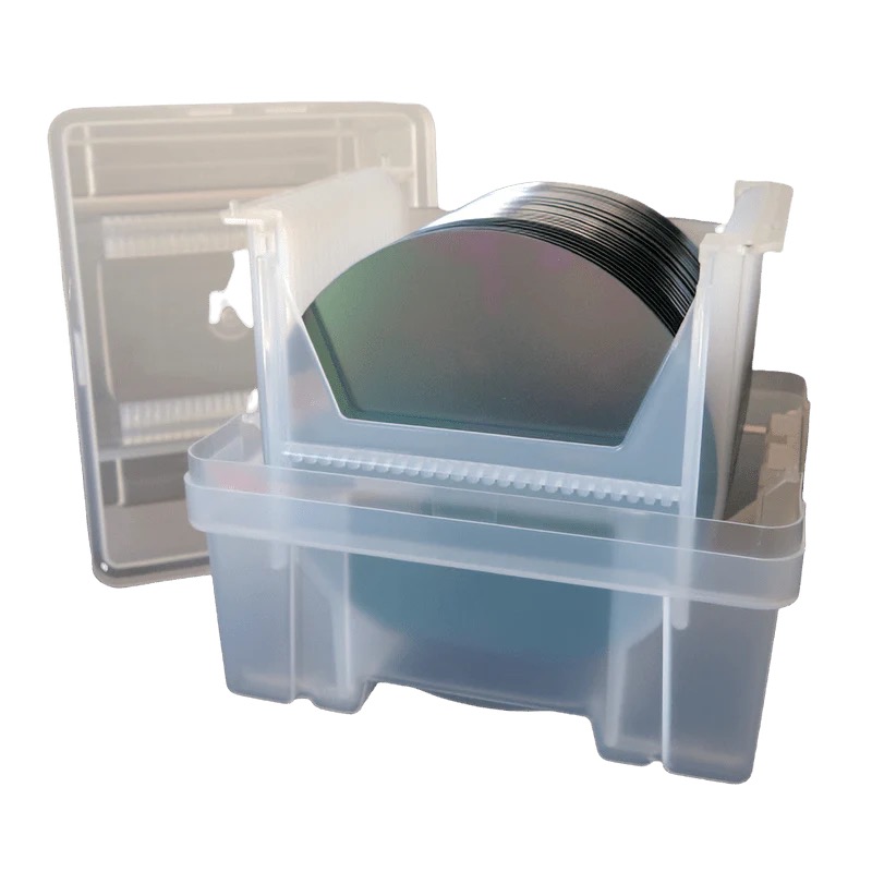
4. Inspection and cleaning: Use tools such as microscopes to check for defects like microtube density and surface roughness. Finally, clean and dry to remove contaminants.
Importance and Challenges
Each step is crucial, especially in controlling crystal defects and dealing with the brittleness of SiC. With the growth of demand, innovative manufacturing processes will help reduce costs and increase output.
Detailed report
A comprehensive analysis of the SiC wafer manufacturing process
Silicon carbide (SiC) wafers have become key components in modern electronics industry due to their superior performance in high-power, high-temperature and high-frequency applications. Especially in the fields of electric vehicles, renewable energy and advanced power electronics, the demand for SiC wafers continues to grow. However, its manufacturing process is complex and challenging, requiring precise materials science and engineering technology. This report elaborately explores each step from crystal growth to final detection, analyzes key technologies and potential issues, and provides supportive information.
The steps and techniques of the manufacturing process
The following are the main steps of SiC wafer manufacturing, based on a comprehensive analysis of multiple reliable sources, including industry websites and academic research:
| Steps | Technology/Method | Description | Key parameters | Challenge |
Crystal growth | Physical Gas phase Transfer (PVT) | High-purity SiC powder is heated to >2000°C, sublimates in a vacuum or inert gas, and condenses on seed crystals to form crystal rods. | Temperature gradient, gas flow rate, impurity level | Control the quality of the crystal and reduce defects such as microtubules and dislocations |
High-temperature chemical vapor deposition (HTCVD) | Thin SiC layers were grown using silane (SiH4) and propane (C3H8) at 1500-1800°C. | Doping concentration, layer thickness | Precise control is carried out to optimize device performance and reduce defect density | |
Crystal rod cutting | - | Use multi-wire cutting equipment to cut the crystal rods into wafers with a thickness of no more than 1mm. | - | To avoid introducing new defects during the cutting process, handle the hardness and brittleness of SiC |
Wafer grinding | - | The wafers are ground with diamond grinding fluids of different particle sizes to achieve the required flatness and roughness. | - | Surface damage and defect introduction |
Polishing | Mechanical polishing (MP) and chemical mechanical polishing (CMP) | The wafer is polished by mechanical and chemical methods to obtain a mirror-like smooth surface, which is suitable for epitaxial growth. | - | Maintain the surface quality and remove residual defects |
Surface preparation | - | Prepare the wafer surface for device manufacturing to ensure there are no defects. | - | Ensure the surface quality before epitaxial growth |
Defect control | - | Optimize the growth conditions (such as temperature and gas flow rate), and use X-ray topographic mapping, photoluminescence mapping, and SEM/TEM detection. Post-processing includes annealing, buffer coating, CMP and reactive ion etching (RIE). | Temperature, impurity level, defect density (<10 microtubules /cm²) | Reduce microtubule, dislocation and stacking failures |
Inspection and cleaning | - | Use tools such as optical microscopes to inspect the microtubule density, surface roughness, resistivity, warpage and TTV (total thickness variation). Clean to remove contaminants and dry with ultra-high purity nitrogen. | Microtube density, surface roughness, resistivity, warpage, TTV | Ensure quality standards and handle residual particles and metal impurities |
In-depth analysis of key technologies
Crystal growth: The core of the PVT method
Youdaoplaceholder0 PVT is the primary method for SiC crystal growth, which involves sublimating SiC powder in a high-temperature vacuum environment and recrystallizing seed crystals. Sources such as Powerway Wafer point out that this process requires high-precision control of the temperature gradient, gas flow rate and impurity level to reduce defects such as microtubules and dislocations. SICC Co.,Ltd. emphasizes that PVT needs to be carried out in a closed space, with limited monitoring, many variables, and extremely high process control accuracy is required.
2.Wafer cutting and processing: Challenges of Hardness and Brittleness
The hardness of SiC is second only to that of diamond, making the cutting process time-consuming and prone to cracking. SemiEngineering's article mentioned that the brittleness and transparency of SiC wafers require special processing equipment, such as new-generation sensors, to prevent damage. Powerway Wafer describes the process of cutting crystal rods into wafers with a thickness of ≤1mm using multi-wire cutting equipment. This step requires careful operation to prevent the introduction of new defects.
3. Grinding and polishing: Guarantee of surface quality
Youdaoplaceholder0 Grinding uses diamond grinding fluids of different particle sizes to ensure smoothness and roughness, while polishing uses MP and CMP to achieve a mirror-finish surface. ScienceDirect's paper proposes a three-step slance-free electrochemical mechanical polishing (ECMP) method, significantly simplifying the traditional process and achieving an atomically smooth surface in less than two hours.
4. Inspection and cleaning: The final checkpoint of quality control
Youdaoplaceholder0 During the testing phase, optical microscopes and instruments are used to check parameters such as microtubule density and surface roughness to ensure compliance with device manufacturing requirements. Clean to remove residual particles and metal impurities, and dry with ultra-high purity nitrogen to avoid contamination. Wevolver's article emphasizes that defect control is a key challenge in SiC wafer production, involving the optimization of growth conditions and post-processing techniques.
Challenges and Future Prospects
The manufacturing of SiC wafers faces multiple challenges, including high costs, high energy consumption and difficulty in defect control. ACM Research pointed out that the growth of SiC crystal rods takes several weeks, while that of silicon crystal rods only takes a few hours, and the cost and energy consumption are significantly higher. In addition, the brittleness and transparency of SiC wafers require special equipment and processing methods, which may affect output and yield.
However, with the growth of demand, the industry is innovating. For instance, NREL's research explores room-temperature aluminum implantation processes to reduce costs and simplify MOSFET manufacturing. Power Electronics News mentioned that X-Trinsic Company focuses on improving wafer manufacturing and recycling to accelerate the market adoption of SiC products. These efforts indicate that in the future, costs may be reduced and efficiency improved through technological progress.
Summary and Significance
The manufacturing process of SiC wafers is the crystallization of materials science and engineering technology, and each step is crucial to the final product quality. From crystal growth to final detection, precise control and innovative technologies ensure the application potential of SiC wafers in the high-power electronics field. With the expansion of the electric vehicle and renewable energy markets, the manufacturing of SiC wafers will continue to be a key focus in the semiconductor industry.