Introduction
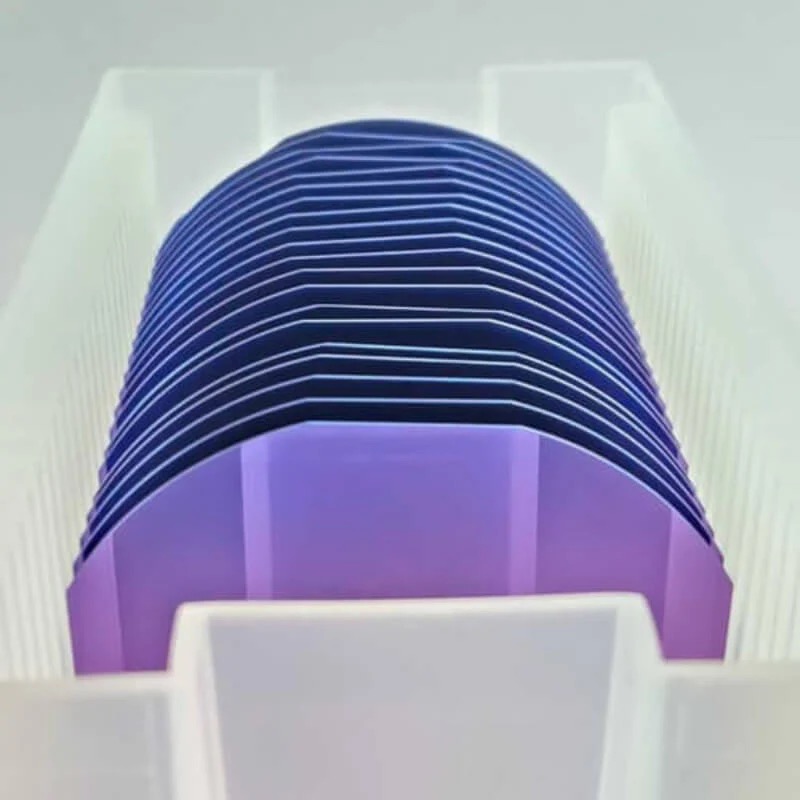
Silicon wafers are pivotal in semiconductor manufacturing, and the 6-inch P/N Type (100) Silicon Wafer with 1~10Ω resistivity and oxide layer offers unmatched versatility for advanced electronics. Combining precise doping, crystal orientation, and a functional oxide coating, this substrate bridges the gap between research innovation and industrial-scale production. This article delves into its specifications, applications, and why it’s a preferred choice for engineers.
Key Specifications
Substrate Design
6-Inch Diameter: Balances cost-efficiency and throughput for IC fabrication, MEMS, and power devices.
(100) Crystal Orientation: Ensures optimal carrier mobility and compatibility with CMOS and photonic devices.
Resistivity Range (1~10Ω)
P-Type (Boron-doped): Ideal for power transistors, solar cells, and high-voltage applications.
N-Type (Phosphorus/Arsenic-doped): Suits high-frequency circuits, sensors, and low-loss devices.
Adjustable doping levels accommodate diverse electrical performance needs.
Integrated Oxide Layer
Thermally grown silicon dioxide (SiO₂) provides insulation, surface passivation, or a dielectric layer.
Enhances device reliability by reducing leakage currents and interface defects.
Advantages of the Oxide Layer
Surface Protection: Shields against contamination during fabrication.
Dielectric Isolation: Critical for gate oxides in transistors and capacitor structures.
Thermal Stability: Withstands annealing and oxidation processes up to 1,100°C.
Why Opt for This Wafer?
Dual Doping Flexibility: Choose P- or N-Type based on device polarity requirements.
Broad Resistivity Range: Adaptable to both high-power and precision analog designs.
Pre-Applied Oxide Layer: Saves time and costs by eliminating additional coating steps.
Industry-Grade Quality: Compliant with automotive, aerospace, and consumer electronics standards.
Conclusion
The 6-inch P/N Type (100) Silicon Wafer with 1~10Ω resistivity and oxide layer is a cornerstone of modern semiconductor engineering. Its adaptable doping, robust oxide integration, and compatibility with cutting-edge applications make it indispensable for innovators in electronics, energy, and microfabrication.
Empower your next project with this high-performance, multi-functional substrate!